|
SBC Circuit Board Assembly and Testing

 Assembling the SBC6120 Assembling the SBC6120
To prepare for the assembly of the SBC, I did the following:
Then, I soldered the components to the PCB, roughly in the following order (it isn’t critical, though):
- Inserted terminals for TP1, 2, 3. I used Vector T68/C miniwrap pins, inserting them with a pair of needle nose pliers. However, lots of other types of terminals would work. (These are not on the parts list.)
- (22) Bypass capacitors. Note that bypass caps are not labeled on the silkscreen. They’re at the notch ends of all chips except U17 and one is shared between U11, U21. Shown in red in Appendix-C of the User’s Manual.
- (8) Resistors, (1 - 4.7K, 7 - 10K)
- Other small components, F1, D1, J11-14, C29-32, 37, U99. Note that the polarity for C29,30,31,21 are shown on the silk with tiny pluses.
 One is opposite from the others. One is opposite from the others.
- S1.
- IC sockets. I used foam as at right to insure they were seated during soldering.
- Connectors.
- J10. Not stuffed until ready to mount on FP board. (See “Mounting the SBC...” below.)
I decided not to try removing the soldering flux, due to the hassle and mild concern that the scrubbing could affect the fine traces and annular rings, which are almost all only 8-mils. It’s pretty much cosmetic, anyway.
The next step was to insert the chips in their sockets. Note that U11 (24-pin “IOT2” device near the 40-pin 6402) points in the opposite direction from the other chips. I should mention that before installing the chips, the manual calls for a power supply test. Also, there is a test with all chips except the CPU. I have skipped these tests here but you might want to consider performing them, as described in Section 2.5 of the User’s Manual.
Bear in mind that these are CMOS parts which are static sensitive. Use of a wrist strap and grounded mat are recommended.  That said, I’ll have to confess that I use little different approach to protecting the chips: I pick up the IC and touch a ground or power pin, then touch a ground-referenced contact on the circuit board. Still holding the chip, I insert it into the socket. The completed SBC board is shown at right. That said, I’ll have to confess that I use little different approach to protecting the chips: I pick up the IC and touch a ground or power pin, then touch a ground-referenced contact on the circuit board. Still holding the chip, I insert it into the socket. The completed SBC board is shown at right.
Jumper Setting
The only jumper needed is across J12, near the power connector. That sets the serial port at 9600 baud. Other settings are: J11 - 38.4kbps, J13 - 1200bps, J14 - 300bps.
Initial Test of the SBC6120
- Connect the IDC-10 female to DB9 male cable to the 10-pin header on the SBC.
- From that cable, connect a DB9 female to DB9 female null modem cable to the serial port on a PC.
- Set a lab power supply for 5VDC, current limited to 400mA. With the supply off, use insulated alligator clip leads to connect it the 4-pin power connector on the SBC. Positive goes to the pin closest to the corner of the board. Negative goes to the pin next to it.
- Run Tera Term or other terminal software on the PC. In the New Connection dialog which appears in Tera Term, select Serial and the COM port which you are using. Press OK.
- On the menu bar, select Setup|Serial Port. Set Port to the COM port you are using. Check the baud rate, which should be 9600 if you placed the jumper across J12. Change Data to 7-bits. Leave Parity and Flow at none.
- Note that if you wish to send a paper tape or other data file to the SBC later, you will need to change Data to 8-bits and may need to set Transmit Delay. I typically use 1msec/char for that. If I’m sending an ASCII program to Focal or Basic, I also use 400msec/line. (I’m not claiming that the delay settings are needed.)
- Turn on the power supply and verify that it isn’t current limiting. You should see the power-on self test (POST) LEDs count through the tests. Facing the four LEDs, only the one on the left (power indicator) and the one on the right should remain on. The one on the right is the LSB of the 3-bit POST code. The 001 code indicates that the monitor software is running. It goes off, if you transfer control to a program in normal memory. (Recall that the monitor code runs in its own memory.) The other POST codes are listed on page-18 of the SBC Manual.
- After the POST passes, you should see the sign-on of the PROM monitor program:
SBC6120 ROM Monitor V320 Checksum 3752 6072 3515 09-APR-10 21:15:39
Copyright (C) 1983-2010 by Spare Time Gizmos. All rights reserved.
NVR: Not detected
IDE: Not detected
IOB: Not detected
- The sign-on indicates that the SBC is working! At the “>” prompt, you could enter commands to deposit values in memory and examine them. The monitor Command Reference starts on page-25 of the User’s Manual.
- I’m pleased to report that my SBC worked on the first try. If yours doesn’t, not to worry—many problems can be solved with these classic solutions:
- Verify your power and terminal connections. (Is the PC’s COM port number correct?)
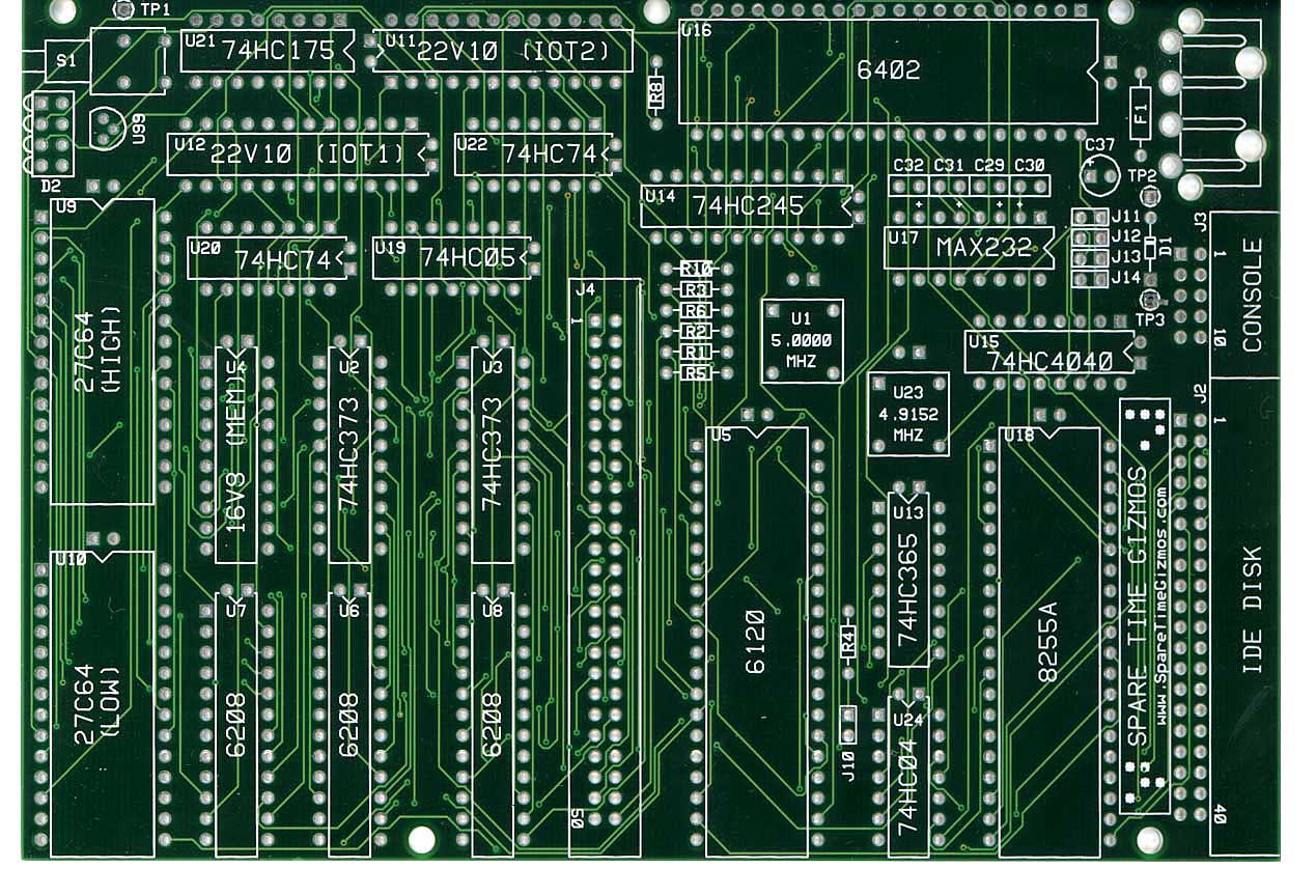
- Check that each chip is in its assigned location and that it’s oriented correctly. PCB photo here.
- Carefully review the solder connections, looking for any solder bridges, splashes, bits of metal or unsoldered joints.
- If the sign-on message appears garbled, it could be because the PC terminal program doesn’t have the port setup for 7-bits, no parity. Check the settings there.
Connecting the Compact Flash “Hard Drive”
 With the power supply turned off, connect the Compact Flash (CF) “Hard Drive” as follows: The details of the cables and adapters used to support mass storage are given in the Parts List. At right, you can see how they are are connected. The CF card resides in the Syba CF to IDE adapter (AD1). Attached to that is the Kinamax 44-pin to 40-pin IDE adapter with power connector (AD2). You can see its power pigtail with green and yellow alligator clips going to it. We need to connect +5VDC power there for the CF. The pin on the end, with a red lead and yellow alligator clip, is positive. A standard 40-pin IDE cable connects AD2 to the SBC. With the power supply turned off, connect the Compact Flash (CF) “Hard Drive” as follows: The details of the cables and adapters used to support mass storage are given in the Parts List. At right, you can see how they are are connected. The CF card resides in the Syba CF to IDE adapter (AD1). Attached to that is the Kinamax 44-pin to 40-pin IDE adapter with power connector (AD2). You can see its power pigtail with green and yellow alligator clips going to it. We need to connect +5VDC power there for the CF. The pin on the end, with a red lead and yellow alligator clip, is positive. A standard 40-pin IDE cable connects AD2 to the SBC.
Though I don’t recall the actual current draw, you may need to increase the power supply limiting to say, 600mA. Turn on the power supply and you should see the monitor software sign-on message as before, except that instead of saying “IDE Not detected,” it should show something like this: IDE: 244MB - TOSHIBA THNCF256MMA
—Of course, yours will show different size, manufacturer and model number details.
Getting the Operating System Running
With that working, we want to transfer an image of the PDP-8/e operating system, known as OS/8, to the CF card. I found that the easiest way to do this is to use a utility created by Steve Gibson, who has a great website section covering the PDP-8/e and SBC6120. His utility, named InstallOS8.exe, contains an image of OS/8. When run from a DOS box under Windows, it will find a CF card which has been previously formatted by the monitor program in the SBC. It then copies the OS/8 image to it. Picking up where we left off on the SBC machine above, here is what you need to do to get OS/8 running:
- NOTE: In working with software on the SBC, always have the CAPS LOCK key enabled. Much PDP-8 software does not understand lower case ASCII.
- In the SBC monitor program, we have just seen it sign-on and recognize the CF/IDE drive as above.
- At the “>” prompt, type the command: DF 0000 (those are zeros, and press Enter). That will format and test partition 0 on the CF card (takes a couple minutes).
- After that completes, power down, remove the CF card and plug it into a CF reader on a PC. Windows will not understand the format and may ask if you want to format the card. Decline that. However, NOTE which drive it has assigned to the card.
- Download InstallOS8.exe here. It’s easier if you put it in a folder, easily accessible at a DOS prompt, such as c:\test.
- Run a DOS box under Windows. One way to do this is to select Start|Run. In the blank field, type: CMD and press Enter. You should see a window filled with black and a DOS prompt.
- If you put InstallOS8.exe in the c:\test folder, at the DOS prompt, type: CD\TEST [press Enter]
 Type: INSTALLOS8 0000 [those are zeros; press Enter] Type: INSTALLOS8 0000 [those are zeros; press Enter]- If it succeeds, you should see some indication of that. If it fails, it will just print usage information.
- Find the icon in your System Tray, which is for “Safely remove hardware.” Right click the icon and select Eject for the drive you noted above as the CF card. If you didn’t note that, run Win Explorer and find the drive with the bad format.
- Remove the CF card from the PC and plug it back in the SBC’s CF adapter.
- Power up the SBC and you should see the monitor sign-on. Type: B [press Enter]
- That should boot OS/8 from the CF card and you should see “–IDA0”, a blank line and simply a dot, for a prompt. IDA0 is the drive name.
- If you see that, type: DIR [press Enter]. After a moment’s pause, it should list the directory as something like the one at right. Please note though, that I have added quite a few files since the original install.
- If you see the directory, CONGRATULATIONS! You have arrived in the rarified atmosphere of the computing elite! :)
- Wanna see it DO something? Okay, let’s run the Focal interpreter. That was a lovable little DEC language, even simpler than Basic. To run it, at the dot prompt, type: R PFOCAL [press Enter]. The “P” comes from OS/8’s original name, PS/8.
- Answer “Y” to the opening question. At the asterisk prompt, enter “TYPE FSIN(3.14)” and it should answer “0.0016”. If you wish, you can enter this simple program. (Type the line numbers, too.):
- 1.1 TYPE " X FSIN(X) FLOG(X) FEXP(X)"
 1.2 FOR X=.1,.1,3; DO 2 1.2 FOR X=.1,.1,3; DO 2
1.3 QUIT
2.2 TYPE ! X,FSIN(X),FLOG(X),FEXP(X)
- Type “GO” to run the program. It should respond with the table at right.
- For some reason, Ctrl-C at the Focal prompt does not return to OS/8, as it’s supposed to. Instead, issue the command: LOGICAL EXIT.
FP Circuit Board Assembly and Testing
Assembling the FP6120
To prepare for the assembly of the FP, I just printed a copy of pages 5-10 of the FP6120 User’s Manual. I then pretty much followed the order of those instructions. Here are some notes on the construction, roughly in that order:
- (Ref manual 2.5.2.) In the group of three photos below right, you can see the switching regulator module, REG1. At the top is the part as delivered, which normally mounts vertically. We need to bend the pins up as shown in the middle picture. The bottom picture shows it mounted on the FP board, with the ferrite core resting on the FP. Actually, there is a horizontal version of the part, but its lead header is mounted on the other side of the board, reversing the pinout from what we need.
The instructions mention socketing RP1 through RP4, in case you might wish to change them to adjust LED current. Since I’m used to running such LEDs at 15mA, the existing current of 5mA seemed low. The main limitation is the max supply current rating of the driver chips. That works out to about 8mA per LED and values of RP1 through RP4 in my Parts List will deliver that. Hence, no RPx sockets are needed. The resulting brightness seems just adequate so I’m glad to have made the change.

- (Ref manual 2.5.3.) As noted above, I left out the PCB power switch and Panel Lock switch and mounted a power switch on the back panel instead. As suggested in the manual, the power switch is wired in series with the back panel power connector and a jumper is soldered at the S1 position on the PCB, as seen at the immediate right. No jumper is needed at the Panel Lock switch position, to eliminate that function.
- (Ref manual 2.5.4.) Since I don’t have the IOB6120 option, I left out the 2-pin header, J4, which would be on the solder side of the FP board. J4 needs to have long leads to reach the IOB and since those would be likely to get bent, it is best installed with the IOB.
Don’t make the mistake that I did, of using the second 50-pin connector provided with the SBC/FP partial kit, at J2 on the FP. The two 50-pin connectors in the partial kit are for J1 in the FP and for the SBC’s J4 (don’t confuse with the FP’s J4, cited in the previous paragraph). Since J2 on the FP supports the IOB, it can remain empty until an IOB option is added. If you do need to populate J2, please see Note-1 in the Parts List.
- (Ref manual 2.5.5.) In case you’re looking for the missing “Figure ??” referred-to in the manual, I’ve provided a photo of the completed FP at the end of this subsection. The instructions envision lining up the LEDs to the end of their barrels, by having the LED flat against the bench. Since my bench has a carpet mat, I used a metal ruler under the LED bar.
The barrel holes in the LED bar assume that the T1-3/4 LEDs have the classic flanges at the base, as seen at right. The ones given in the parts list do have the flanges, so will work fine. The ones I ordered before I knew about that, came without flanges and as a result, looked off-center in their holes. Wanting my unit to look nice, I added rings of #24 bus wire around the LEDs, to center them. The series of four pictures below the Flange pic show the sequence of winding, cutting and affixing suitable rings. That did fix the centering problem, as seen in the last frame of the series. Again, you should not need to worry about making rings, if you use the LEDs in the parts list given in Part I of this article. Typo correction: there are 28 LEDs, rather than the 26 mentioned in the instructions.
- (Ref manual 2.5.6.) For reference, here is a list of the momentary switches (as labeled on the FP board):
- DEP (the only one pointing down in rest position)
- EXAM
- CONT
- CLEAR
- LXA
- LX
- BOOT
Regarding cutting the switch shaft: The instructions say that the shaft should be cut to roughly 0.4”. I used a different knob than the original, substituting the Radio Shack 274-415A. It’s depth, from the bottom of the skirt, is 0.375”. The actual length I cut it to was 0.402” and that came very close to giving the desired 0.05” clearance from the knob to the panel.
The method I use to cut accurately, is to mark the cut and put the end of the shaft in a drill press. With the drill running, I hold a utility knife against the plastic shaft at the mark, resting my hands on the nearby drill press table. This typically cuts within 10mils or so of nominal. Your mileage might vary, so it’s often a good idea to cut it a little long and grind it down.
 I’d like to amplify the manual’s comment about keeping the tang washer on the switch: With the nut off, it’s very easy to forget that the tang washer isn’t attached and lose it. Happened to me and I wound up making the replacement tang at left. I did end up finding the original one. I’m glad I found it, because the DIY version stopped a little beyond the last click. The factory version doesn’t go straight in the hole, as I had supposed. Instead, it angles outward from the axis of the switch. That results in the switch stopping at a different position for a given tang position and it works better. I’d like to amplify the manual’s comment about keeping the tang washer on the switch: With the nut off, it’s very easy to forget that the tang washer isn’t attached and lose it. Happened to me and I wound up making the replacement tang at left. I did end up finding the original one. I’m glad I found it, because the DIY version stopped a little beyond the last click. The factory version doesn’t go straight in the hole, as I had supposed. Instead, it angles outward from the axis of the switch. That results in the switch stopping at a different position for a given tang position and it works better.
- We need to drill-out the threads of the swages of the IDE Drive Position (ref photo below). That’s because the drive requires screws from underneath and they are metric M3 x 12mm, as specified in the Parts List. You can use a 1/8” drill bit, which might be a little tight. Either wobbling it a little or using a 9/64” bit should work.
- The next step in assembling the FP6120 is to install the chips in their sockets. Photos of the finished FP front and back, are presented below.


Attaching the Faceplate
Because mounting the SBC and IDE Drive will block three screw holes (as seen above), we need to attach the faceplate to the FP before testing it. Of course, should something be wrong, you might need to remove the faceplate to debug the problem, though. With the faceplate face-down on something which won’t scratch it, align the FP with the mounting posts and fasten with eight, 4-40 screws and lock washers. 3/16" screws are provided with the partial kit but after going through the PCB, they fall short of the minimum three turns of purchase. Hence, I used 1/4” screws.
Mounting the SBC Board and Compact Flash on the FP Board
We are now ready to integrate the SBC and FP boards. Find the five swages on the bottom of the FP board, under the SBC Board Position, as shown in the photo above. Screw-in the five, nylon, male/female spacers (specified in the Parts List) into the swages. Do not over-tighten. Position the SBC on the spacers, with its components facing the bottom of the FP. Make sure that all of the pins from the FP are properly inserted into the expansion connector on the SBC. Fasten the SBC to the spacers with the five nylon screws. Do not over-tighten.
Installing J10 in the SBC
J10 is a pair of long pins to be soldered to the SBC, which mate with J5 on the bottom of the FP board. You can see J5 in the photo above, as the small, 2-pin female header on the right side of the SBC Board Position. As mentioned in Note-8 of the Parts List, J10 is supplied as a 4-pin header and you need to chop off two of the existing pins. I use diagonal cutters to cut these headers. Beware that they can crack, so it’s best to cut closer to the part you will discard, than the part you want to keep. With the SBC still mounted on the FP, insert the two pin header from the the back of the SBC board. You can locate it as the only pair of unsoldered holes in that area of the PCB. Insure that both pins are firmly inserted into the mating connector on the FP. Solder the pins and cut off the excess, including the plastic part.
 Modifying the CF/IDE Drive (hereafter “CF Drive”) Power Connection Modifying the CF/IDE Drive (hereafter “CF Drive”) Power Connection
[Ref notes 3 and 16 in the Parts List.] The 44-pin to 40-pin IDE adapter cable (AD2 in the Parts List) includes a Molex connector power connection to support the drive. We will be attaching that to the power connector on the SBC but it’s the wrong sex. I included a disk drive power Y-adapter in the Parts List to act as a donor for the proper connector. Cut a female connector from the Y-adapter and replace the male power connector of the 44-pin to 40-pin IDE adapter, AD2. Match the red and black wires and clip off the extra wires of the donated connector, as shown.
 Mounting the CF Drive on the FP Mounting the CF Drive on the FP
You could hold off mounting the CF drive until after the FP is tested but we will cover it here. In any case, connect its IDE cable and power cable to the SBC. Locate the four swages for mounting the IDE drive on the back of the FP board. Having drilled-out the threads of the swages, as covered above, mount the CF drive using four M3 x 12mm screws. Note that one of the screw locations is partially obstructed on the front of the FP by the LED bar, as seen in the photo at right. It only required a little carving with a Dremel cutter to fit the screw in.
The fully assembled electronic system is shown below (sans faceplate). Sharp-eyed readers might notice that metal screws are used to fasten the SBC, instead of the nylon ones specified in the Parts List. The reason is that I used a shorter connector for the SBC J4 and needed to use shorter (unthreaded) standoffs to lower the SBC on the FP board. A long metal screw was used to fasten directly to the swages. Notice that two screw positions needed fiber washers to protect nearby PCB traces. Although the short connector caused a mechanical hassle, it did have the good outcome that the hardware supporting the SBC is now much stronger than the 4-40 nylon screws and spacers. Nylon can crack over time, so you should be careful not to tighten the SBC mounting screws and spacers more than necessary.

Testing the SBC/FP System
[Ref “Initial Test...” above.] Connect the PC/terminal serial line to the SBC. Connect a power supply to the FP DC jack. Upon applying power, the SBC should go through self test and you should see the monitor sign-on at the terminal, as before. During self test, the FP lights will flash and all will come on briefly.
Set the HALT switch up, the rotary switch to MD (Memory Data) and the switch register (hereafter “SR”) to all ones (switches up). Momentarily depress ADDR LOAD and all Memory Address (hereafter “MA”) LEDs should light up. All Data LEDs (hereafter “DD”) will also light up, indicating that the value in address-7777 is all ones. [Traditionally, PDP-8 address and data values have been designated with octal notation, which we use here.] During the power-on self test, the monitor software writes each location with its address. Press (and release) EXAM a few times. MA will increment (first rolling over to address-0000) and DD will show the same thing, due to the preset values.
Wanna toggle-in a quick program, just like REAL MEN used to do? :) Here’s an echo program, which accepts characters from the serial port and echos them back. It needs to be loaded, starting at location 0200. To do that, set the SR to 0200 and press ADDR LOAD. Set SR to 6040 and press DEP up, momentarily. That loads the first instruction and increments MA. Continue with the rest of the instructions in the DATA column below.
 ADDRESS DATA INSTRUCT COMMENT ADDRESS DATA INSTRUCT COMMENT
0200 6040 TFL /set TX flag initially
0201 6032 KCC /clear RX flag and AC
0202 6031 KSF /skip on RX flag
0203 5202 JMP /check flag
0204 6036 KRB /RX=>AC 4-11, clear RX flag
0205 6041 TSF /skip on TX flag
0206 5205 JMP /check flag
0207 6046 TLS /AC4-11=>TX, clear TX flag, AC
0210 5202 JMP /get next char at locn 0202
After entering the program, set SR to 0200 and press ADDR LOAD. With your terminal program still running on the PC press CLEAR and then CONT (under the START label). The RUN LED should light. Type on the PC keyboard and you should see the characters echoed to the screen. Congratulations, now you know what it feels like to be a REAL MAN! :-D
Assuming that you’re not too drunk with computing power, you should go ahead and verify that the operating system still boots. You can do that now by setting the HALT key down and back up, then pressing the BOOT switch (lower left of the front panel) twice. You should see the dot-prompt of OS/8. Typing DIR [Enter] should list the files in the directory. Problems?—Did you remember to set the serial port in Tera Term for 7-bits? Did you remember to put the Caps Lock key on?
Note about what we did with the HALT key before the boot: We needed to take the system out of Run mode to get the monitor program reactivated and looking at the front panel hardware. Setting the HALT key down did that. We then needed to set it back to the up position, to allow OS/8 to run, after pressing BOOT twice.

<<< Return to Part I - Overview, Documentation and Parts
Now at Part II - PCB Assembly, Software and Testing
Continue with Part III - Building the Enclosure >>>
Jump to Part IV - Final Assembly and Support Software >>>
Copyright © 2013 by Stephen H. Lafferty. All rights reserved.
_
|


